

")
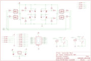
We start with the schematic - connecting all the various elements of the circuit together, and verifying it using design verification rules.
Several revisions of design may be undertaken to perfect it.
Wherever possible, we try to make any prototypes modifyable - so if something was not anticipated - such as new features being added - the prototype can be modified to suit.
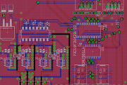
While it is possible to complete the schematic first, and then go on to the PCB design, we often make the PCB design integral with the schematic design - especially if the components being used have generic pins available for use. This allows us to create the optimum layout for the circuit.
During the layout process, design verification rules will be frequently executed to make sure that there will be no problems making the circuit board.
In addition, if it's possible to make it easy to modify the circuit once manufacturered, then we'll incorporate it into the design - such as adding test points, or break-out points.
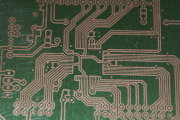
Manufacturing the PCB is the next stage - our in-house prototype facilities are geared towards single layer PCB (and this is where we would always try to start), but we can do two-layer non-PTH boards.
We use photo-lithographic methods to produce the boards - so there is a developer chemical and etching chemical used for the main PCBs, and after the etching and drilling, they are chemically tinned to produce a circuit board that will be longer lasting, easier to solder, and looks good.
Our in-house facilities can cope with 0.5mm spacing found on many available QFP packages, and we have been successful with 0.4mm spacing (although it is pushing our current lithography capabilities - so we would prefer not to have to go down to that level!).
For anything that we are unable to cope with in-house (such as higher density, PTH, multi-layer, solder resist, silk screen), then we would use an outside PCB production company to manufacture the boards for us - although this has an additional lead time.
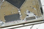
With the PCB manufactured, the components are soldered on the board. We generally use a soldering iron with a moderately fine tip on it (1x0.8mm), but we also have hot-air SMT rework capability, so if components need to be removed or resoldered, it can be done with hot air.
We also have access to a pick-and-place machine, and a reflow oven, so if a design requires a denser board, or some more complicated components soldered to the board (such as QFN or DFN), then we can do it.
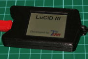
In some cases, an enclosure is needed for the prototype - we can either use an off-the-shelf aluminium case (in which case we'll try to design the PCB to fit optimally), or we can design a case and print it using our 3D printer - in which case the size of the PCB is less relevant.
Here is a short list of some of the projects we have worked on: